
Technology
Pyramidal MicroLEDs, grown bottom-up
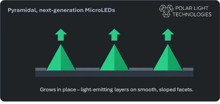
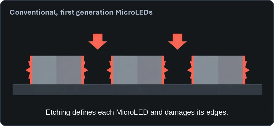
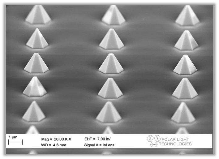
Our MicroLEDs are hexagonal InGaN/GaN pyramids grown bottom-up from the epi-wafer instead of being etched out of a planar epi stack, top-down. This gives excellent surfaces without etching damage, crucial for optoelectronic performance, in particular as dimensions shrink.
Technical characteristics
What bottom-up growth gives
| Architecture | Hexagonal GaN pyramids with InGaN quantum wells as the active light-emitting region, grown bottom-up instead of etched out of a planar epi stack |
|---|---|
| Size | Pyramidal nanoLEDs demonstrated down to 450 nm |
| Position, density and shape | Deterministic, defined by the growth mask |
| Surface | Excellent surface smoothness due to the bottom-up growth. No etching damage on the sidewalls |
| Strain | The geometry of the pyramids results in less strain, which increases the ability to get more indium into the quantum wells, i.e. of increasing importance with longer wavelengths |
| Piezoelectric field | Reduced effect, due to the pyramid base angle, meaning faster recombination time and more photons per time unit (i.e., higher data bandwidth) |
| Emitting area | The emitting facet area is more than double, 113% larger, than the pyramidal base area (7.38 µm² against 3.46 µm²) |
| Light lobe | Lambertian |
| Integration | Flip-chip integration proven |
Grown, not etched
Two ways to make a MicroLED
Development
What has been shown, and when
First blue and green pyramidal MicroLEDs
Red in the same InGaN/GaN material system
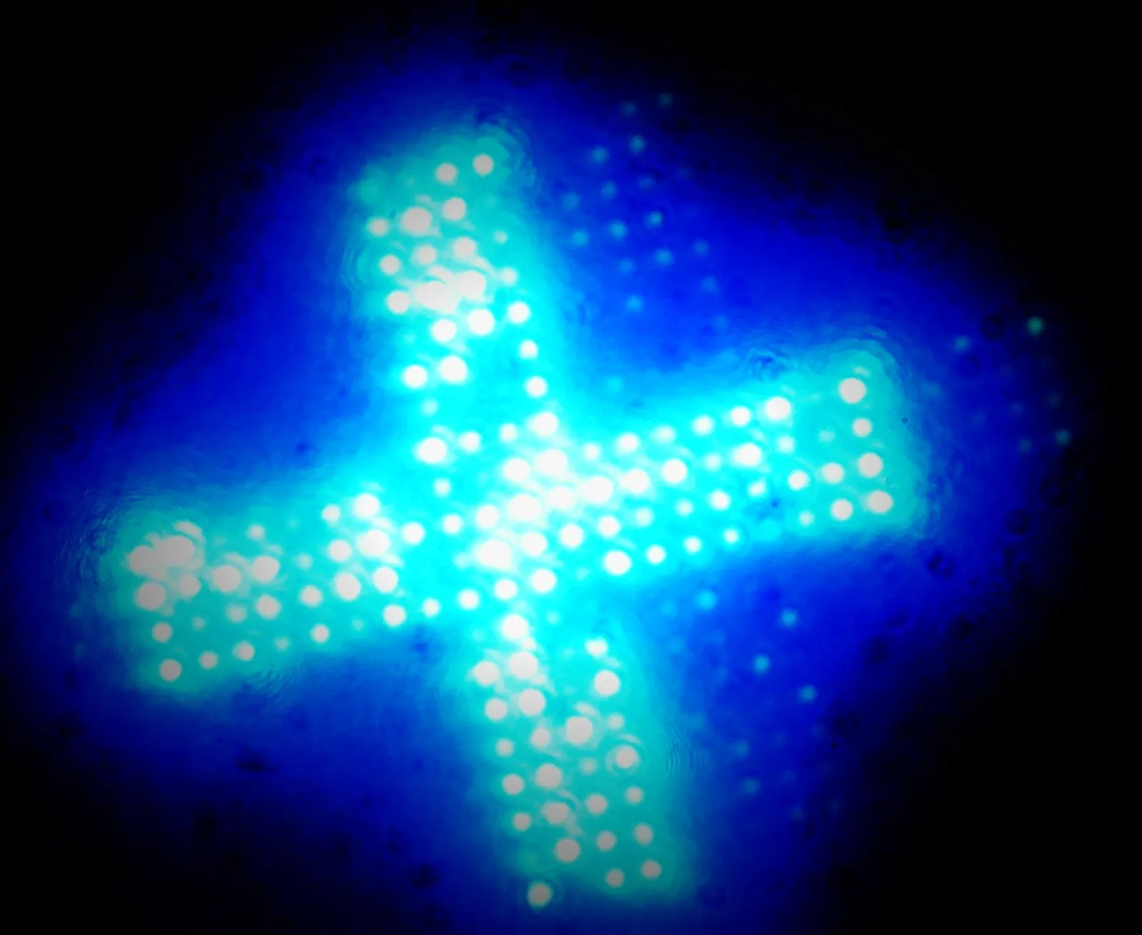
First working pyramidal MicroLED based display
First working blue and green pyramidal MicroLED based display
NanoLEDs with size of 450 nm demonstrated
Demonstrated on the same architecture. Not today’s offering.
First MicroLEDs on a manufacturing pilot line
Produced at VTT Technical Research Centre of Finland.
Publications
Pyramidal GaN research
Ten peer-reviewed papers, 2011 to 2022, from the Linköping University research the company grew out of.
GaN-based light-emitting materials prepared by hot-wall metal-organic chemical vapor deposition
Son Phuong Le, Chih-Wei Hsu, Ivan Martinovic, Per-Olof Holtz
GaN-based pyramidal quantum structures for micro-size light-emitting diode applications
Son Phuong Le, Chih-Wei Hsu, Ivan Martinovic, Per-Olof Holtz
Polarized single photon emission and photon bunching from an InGaN quantum dot on a GaN micropyramid
Tomas Jemsson, Houssaine Machhadani, Per-Olof Holtz, K Fredrik Karlsson
Direct generation of linearly polarized photon emission with designated orientations from site-controlled InGaN quantum dots
Anders Lundskog, Chih-Wei Hsu, K Fredrik Karlsson, Supaluck Amloy, Daniel Nilsson, Urban Forsberg, Per Olof Holtz, Erik Janzén
Linearly polarized single photon antibunching from a site-controlled InGaN quantum dot
Tomas Jemsson, Houssaine Machhadani, Per-Olof Holtz, K Fredrik Karlsson, Chih-Wei Hsu
Deterministic Single InGaN Quantum Dots grown on GaN Micro-Pyramid Arrays
Per Olof Holtz, Chih Wei Hsu, Anders Lundskog, K. Fredrik Karlsson, Urban Forsberg, Erik Janzén
Morphology Control of Hot-Wall MOCVD Selective Area Grown Hexagonal GaN Pyramids
Anders Lundskog, Urban Forsberg, Per Olof Holtz, Erik Janzén
InGaN quantum dot formation mechanism on hexagonal GaN/InGaN/GaN pyramids
A Lundskog, J Palisaitis, C W Hsu, M Eriksson, K F Karlsson, L Hultman, P O Å Persson, U Forsberg, P O Holtz, E Janzén
Controlled growth of hexagonal GaN pyramids by hot-wall MOCVD
Anders Lundskog, C.W. Hsu, D. Nilsson, K.F. Karlsson, U. Forsberg, P.O. Holtz, E. Janzén
Single Excitons in InGaN Quantum Dots on GaN Pyramid Arrays
Chih-Wei Hsu, Anders Lundskog, K. Fredrik Karlsson, Urban Forsberg, Erik Janzen, Per Olof Holtz